The 160GB Memory Compromise: Unpacking Intel’s Leaked Xe3P Core Architecture
For the past year, the artificial intelligence hardware market has been strangled by a single, catastrophic bottleneck: High-Bandwidth Memory (HBM). Nvidia’s massive enterprise GPUs require it, AMD’s Instinct accelerators require it, and the global supply chain simply cannot produce enough of it to satisfy the hyperscale data centers. This shortage has driven hardware costs to astronomical levels, pricing out smaller enterprises and developers looking to run massive local Large Language Models (LLMs).
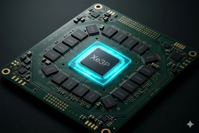
Enter Intel. Following months of speculation regarding the future of their dedicated graphics division, a monumental leak has surfaced. High-resolution PCB images of Intel’s upcoming “Crescent Island” data center accelerator have hit the web, revealing the highly anticipated Xe3P core architecture.
However, it is not the raw compute power that has the industry buzzing; it is Intel’s radical, highly pragmatic memory configuration. By entirely abandoning HBM in favor of a staggering 160GB of LPDDR5X memory, Intel is attempting to sidestep the supply crisis entirely. Here is the comprehensive, deep-dive breakdown into the Xe3P leak, the fascinating bandwidth math behind the Crescent Island accelerator, and why this “compromise” might be the smartest engineering decision Intel has made in years.
Crescent Island: The First Look at Xe3P
To understand the magnitude of this leak, you must first understand where Xe3P fits into Intel’s broader silicon roadmap.
While the standard Xe3 (Celestial) architecture is slated to power the integrated graphics inside upcoming consumer processors like Panther Lake, the “P” in Xe3P denotes Performance and extreme scalability. This is not a consumer gaming card. The Crescent Island PCB leak confirms that Intel is prioritizing the enterprise and workstation markets over the enthusiast desktop segment for this generation of dedicated silicon.
A Massive Die: The leaked PCB layout, courtesy of hardware insider YuuKi_AnS, reveals a socket designed for an absolutely massive Xe3P logic die, visually dwarfing the current Battlemage generation.
The Single 16-Pin Connector: Power delivery is handled by a single, rear-mounted 16-pin connector. This confirms that the Crescent Island board is designed to pull up to 600W of sustained power, placing it firmly in the heavy-compute tier alongside Nvidia’s flagship offerings.
Workstation Form Factor: The presence of 13 populated VRM stages (out of 18 total pads) and a standard PCIe form factor indicates this card is intended to slot directly into workstation towers and localized AI servers, rather than relying exclusively on specialized NVLink-style backplanes.
The HBM Crisis and the LPDDR5X Workaround
The defining feature of the Crescent Island board is what is absent: there are no silicon interposers for High-Bandwidth Memory. Instead, Intel has engineered a brilliant, brute-force workaround to the global HBM shortage.
Sidestepping the Bottleneck
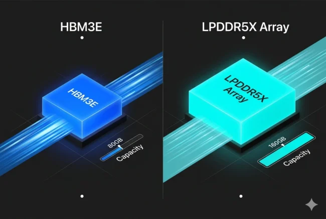
The Cost of HBM: Securing HBM3E for modern AI accelerators currently accounts for a massive percentage of the Bill of Materials (BOM). Nvidia’s memory costs have reportedly soared 485% year-over-year. By refusing to use HBM, Intel instantly cuts the manufacturing cost of Crescent Island by thousands of dollars.
The 20-Pad Array: The leaked PCB reveals 20 distinct physical memory solder pads surrounding the GPU socket—12 on the front of the board and 8 on the rear.
The 160GB Milestone: These pads are designed to house high-density LPDDR5X modules. By populating all 20 sites with 8GB packages, Intel achieves an incredible 160GB of total VRAM. This capacity eclipses the current 80GB and 96GB standards found on many high-end enterprise cards, providing a massive buffer for AI workloads.
The Bandwidth Math: Trading Speed for Capacity
LPDDR5X is inherently slower than HBM. To prevent the Xe3P core from starving for data, Intel has drastically widened the memory interface.
The Bus Width: Utilizing 20 individual memory packages implies an incredibly wide memory bus. If Intel utilizes a 32-bit connection per package, the board features a 640-bit wide interface. However, advanced leaks suggest Intel may be utilizing 64-bit LPDDR5X packages, which would result in a monstrous 1280-bit memory bus.
1.5 TB/s Throughput: Running high-binned LPDDR5X at 9600 MT/s across a 1280-bit bus mathematically yields approximately 1.5 Terabytes per second (TB/s) of memory bandwidth.
The Compromise: While 1.5 TB/s is roughly half the bandwidth of Nvidia’s highest-tier HBM accelerators, it perfectly matches the throughput of high-end workstation cards like the RTX 6000 Ada Generation. Intel is essentially sacrificing peak theoretical bandwidth to deliver double the memory capacity at a fraction of the retail cost.
Unpacking the Xe3P Architecture
The sheer size of the Crescent Island socket indicates that the Xe3P architecture is built for extreme parallel compute. While the exact core counts remain guarded, the scaling math from Intel’s consumer division paints a vivid picture.
Scaling Up from Panther Lake
The iGPU Baseline: We know that the upcoming Panther Lake and Nova Lake consumer processors will feature up to 12 Xe3 / Xe3P cores. In those low-power envelopes, Intel claims a 20% to 25% architectural performance uplift over the previous generation.
The Enterprise Multiplier: The Crescent Island Xe3P die is radically larger than a mobile iGPU. Architectural analysts estimate the die will house between 32 and 64 Xe3P Compute Blocks.
Dedicated AI Hardware: Like all modern architectures, Xe3P is heavily optimized for inference. The silicon will feature dedicated matrix multiplication units designed to natively accelerate INT8, FP16, and the crucial FP8 data types required for modern generative AI software.
The Local LLM Dream Machine
For the hardcore AI enthusiast, localized enterprise developer, and the r/LocalLLaMA community, the Crescent Island leak represents a holy grail piece of hardware.
Why Capacity Trumps Speed in Inference
The VRAM Wall: Running Large Language Models locally is entirely dictated by VRAM capacity. If a model’s weights exceed your graphics card’s memory, the system must offload data to the vastly slower system RAM, plummeting token generation speeds from 50 tokens-per-second to 2 tokens-per-second.
Running the 300B Behemoths: A 160GB VRAM buffer allows a developer to load massive, 300-billion parameter open-source models (quantized to 4-bit) entirely into the GPU’s memory. Currently, achieving this requires networking multiple RTX 4090s or 3090s together via PCIe risers—a buggy, power-hungry nightmare. Crescent Island handles it on a single board.
The Cost Disruption
If Intel prices the Xe3P Crescent Island card aggressively—analysts project a potential MSRP in the $10,000 to $16,000 range—it will severely undercut Nvidia’s enterprise monopoly. It offers a mid-tier bandwidth solution with top-tier VRAM capacity, making it the most cost-effective inference accelerator on the global market.
What This Means for Intel’s Future (and PC Gamers)
The brilliance of the Xe3P LPDDR5X strategy comes with a bitter pill for traditional PC gamers.
The Death of Consumer Arc Celestial?
The resources required to validate and mass-produce a 1280-bit, 160GB AI accelerator are immense. The current rumors heavily suggest that Intel is prioritizing this lucrative data center market at the expense of releasing dedicated high-end consumer gaming cards based on the Xe3 architecture.
If you were waiting for an “Arc C770” to compete with the RTX 5070, you will likely be disappointed. Intel’s strategy for consumer gaming appears to be fully pivoting toward ultra-powerful integrated graphics (iGPUs) on their Nova Lake desktop CPUs, while leaving the high-end discrete GPU market to Nvidia and AMD.
The Verdict: A Masterclass in Pragmatism
In the semiconductor industry, brute force rarely wins against clever engineering. By recognizing that they could not outbid Nvidia for limited TSMC packaging and HBM supply, Intel did the smartest thing possible: they changed the rules of the game.
The Crescent Island Xe3P accelerator is a masterclass in pragmatism. By utilizing 160GB of high-speed LPDDR5X smartphone and laptop memory, Intel has engineered a 600W inference monster that delivers the exact specification AI developers are begging for—massive capacity—while entirely bypassing the supply chain crisis holding the rest of the industry hostage. When it launches in the second half of 2026, it has the potential to fundamentally democratize the local AI landscape.