Are 2nm Chips Actually Efficient? Unpacking the 100W Charging Reality of Modern Androids
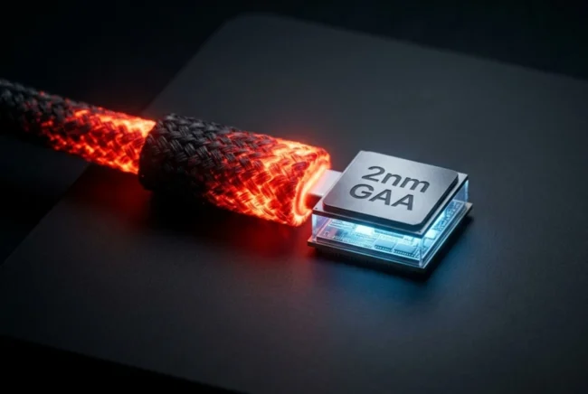
The semiconductor industry’s marketing machine is relentlessly focused on miniaturization. In 2026, we have officially crossed the threshold into the “Angstrom Era,” with TSMC and Samsung spinning up their bleeding-edge 2-nanometer (2nm) fabrication nodes. The central promise of this architectural leap—plastered across every keynote and press release—is revolutionary power efficiency.
Yet, a glaring paradox exists in the modern Android ecosystem. If these 2nm chips are genuinely the most energy-efficient silicon ever designed, why are the flagship smartphones of 2026 thicker than ever? Why are manufacturers scrambling to implement massive 6000mAh+ Silicon-Carbon batteries, and why are we entirely reliant on aggressive 100W to 120W fast-charging bricks just to make it through a heavy day of use?
The reality of 2nm efficiency is far more complicated than the marketing suggests. It involves a fundamental misunderstanding of how performance metrics are measured, the brutal thermal realities of high-speed charging, and an industry obsessed with benchmark scores over practical endurance. Here is the comprehensive breakdown of the 2nm efficiency illusion and the 100W charging reality.
The 2nm Promise vs. Peak Power Reality
To understand why our phones are still draining quickly, you must first understand the specific, highly conditional definitions of “efficiency” used by silicon foundries.
The “Iso-Performance” Catch
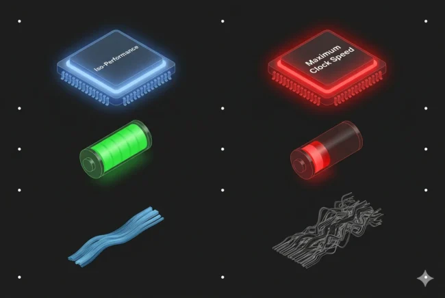
The Baseline Metric: When TSMC claims its N2 (2nm) node uses “25% to 30% less power,” there is a massive, unspoken asterisk attached: this is at iso-performance.
The Translation: This means that if you took a 2023 smartphone chip running at its standard clock speed and recreated it on a 2nm node, it would draw 30% less battery.
The Reality of Scaling: However, smartphone manufacturers (Qualcomm, Samsung, and Apple) never keep performance static. They use the power savings generated by the 2nm node to aggressively push clock frequencies higher. They reinvest the efficiency gains back into raw performance. As a result, the new chip draws the exact same—or often more—total power than the previous generation, it just completes calculations faster.
The Gate-All-Around (GAA) Architecture
Solving FinFET Leakage: For over a decade, chips relied on FinFET designs, where the gate surrounded the transistor channel on three sides. At ultra-small scales, electricity began to “leak” out the fourth side, generating wasted heat and killing battery life.
The 4-Sided Solution: 2nm introduces the Gate-All-Around (GAA) nanosheet design, wrapping the gate completely around the channel. This provides total electrostatic control, drastically reducing passive power leakage when the phone is idle.
The Active Load Paradox: While GAA makes 2nm chips incredibly efficient while idling in your pocket, that efficiency curve shatters when the processor is pushed to maximum load.
The 30W Benchmark Nightmare
Exynos 2600 Testing: Recent independent testing of Samsung’s flagship 2nm GAA chip, the Exynos 2600, revealed a terrifying reality. During Geekbench 6 multi-core stress tests, the AP hit a peak power draw of 30.22W. This is a wattage typically reserved for ultrabook laptops, not passively cooled smartphones.
Snapdragon’s High Baseline: While more efficient than Samsung, the upcoming Qualcomm Snapdragon 8 Elite Gen 6 on TSMC’s 2nm node is still routinely pulling over 20W in peak burst scenarios.
The Battery Drain: When a smartphone chip demands 20W to 30W of power to render a heavy game or process a localized AI language model, even a massive 6000mAh battery will be depleted in a matter of hours. The silicon is faster, but it is undeniably power-starved.
Why 100W Charging is a Necessary Band-Aid
Because semiconductor designers refuse to cap peak clock speeds, smartphone OEMs are left trying to mitigate the resulting battery drain. Their primary solution is not extending battery life, but minimizing the downtime when the battery inevitably dies.
Combating the Burst Drain
The Rise of Agentic AI: Modern 2026 smartphones run continuous background AI tasks—analyzing screen context, processing voice data, and generating images locally. These workloads utilize the Neural Processing Unit (NPU) heavily. These constant “bursts” of extreme compute power chip away at the battery capacity much faster than traditional app navigation.
The “Topping Up” Culture: Instead of engineering a phone that lasts two full days of heavy use, Android manufacturers have conditioned the market to accept “topping up.” Implementing a 100W or 120W charging infrastructure allows a user to plug in their dead phone and reach 50% capacity in under 10 minutes.
Masking the Inefficiency: High-wattage charging acts as a psychological band-aid. If your phone charges in 15 minutes while you take a shower, you are less likely to notice or care that the 2nm processor is actually highly inefficient under load.
The Dual-Heat Problem: Fast Charging Meets 2nm Density
Combining highly dense 2nm processors with 100W charging bricks creates the most significant engineering challenge of the decade: catastrophic thermal overlap.
Thermal Constraints in a Glass Sandwich
Transistor Density Trap: A 2nm processor packs significantly more transistors into a smaller physical die area than a 3nm or 4nm chip. When this dense cluster is forced to run at 5.0GHz, it creates a massive, concentrated thermal hotspot that is incredibly difficult to dissipate.
The 100W Thermal Load: Pushing 100 watts of electrical current into a smartphone battery generates immense ambient heat, regardless of how efficient the external Gallium Nitride (GaN) charging brick is.
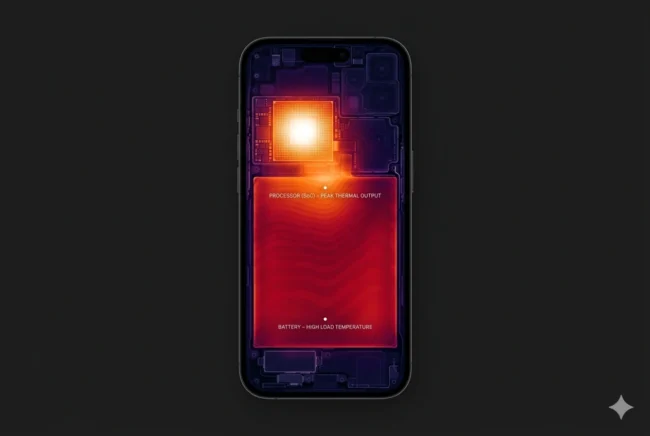
The “Double Heat” Scenario: If a user attempts to play a heavy game (pushing the 2nm chip to its 20W+ peak) while the phone is plugged into a 100W fast charger, the smartphone experiences a “double heat” event. The logic board and the battery both emit extreme temperatures simultaneously.
Battery Degradation and Throttling: Lithium-ion and newer Silicon-Carbon cells degrade rapidly when exposed to sustained temperatures above 45°C. To prevent the battery from swelling or the screen from burning the user, the device’s firmware must aggressively throttle the 2nm processor, ruining the gaming performance the user paid a premium for.
TSMC N2 vs. Samsung SF2: The Efficiency Divide
It is important to note that the 2nm reality is not identical across the industry. A massive divide has opened between the world’s two leading foundries, dictating which Android phones survive a heavy workload and which ones overheat.
Not All 2nm is Created Equal
Samsung’s Yield and Heat Struggles: Samsung’s Foundry has aggressively pushed its SF2 node, but real-world testing of the Exynos 2600 shows it trailing its TSMC equivalents by up to 28% in battery life tests. The architecture relies on aggressive core configurations to win benchmark scores, sacrificing sustained thermal efficiency.
TSMC’s Thermal Discipline: TSMC’s N2 node, which powers the upcoming Apple A20 Pro and the highest-tier Snapdragon chips, displays far better thermal discipline. However, TSMC is constrained by what its clients demand. If Qualcomm demands a 5.0GHz clock speed, TSMC will print it, resulting in the high power draws we are seeing.
The Apple Advantage: Apple’s approach to TSMC’s 2nm node is markedly different from the Android ecosystem. By utilizing advanced Wafer-Level Multi-Chip Module (WMCM) packaging and strictly capping peak clock speeds, the A20 Pro spreads heat more effectively. Apple prioritizes an isolated thermal envelope over chasing maximum Geekbench scores, allowing for cooler fast-charging sessions.
The Path Forward: Thermal-Smart Ecosystems
The industry is beginning to realize that pushing raw wattage through a wall charger and cranking clock speeds on a tiny silicon die is an unsustainable strategy.
Beyond Raw Wattage
Intelligent Charging Protocols: Premium 2026 devices are moving away from “dumb” 100W charging. Modern GaN chargers now communicate directly with the smartphone’s internal temperature sensors via adaptive power delivery algorithms. If the 2nm chip crosses a thermal threshold, the charger instantly steps down from 100W to a manageable 25W.
Hardware-Level Cooling Integration: As we explored in previous deep-dives, technologies like Qualcomm’s Heat Pass Block (HPB) are becoming mandatory. To survive the 2nm era, the processor packaging itself must be actively designed to route heat immediately into the phone’s vapor chamber, rather than letting it soak into the battery housing.
The End of the Wattage Race: Consumers must look past the marketing numbers. A processor that scores 3.5 million on AnTuTu is useless if it throttles after five minutes, and a 120W charger is a liability if it degrades the battery within a year.
The 2nm node is an incredible piece of human engineering, but it is not magic. Until smartphone manufacturers stop prioritizing peak theoretical performance over sustained, thermal-efficient operation, the 100W charging brick will remain a mandatory crutch for an industry that refuses to slow down.
Tech ReviewerFounder & Publisher: Sole operator and lead technical architect of MultiCore Performance
Areas of Expertise:
Silicon & Hardware Benchmarking: Firsthand performance testing and analysis of flagship processors specifically evaluating thermal and rendering capabilities in gaming and video editing workloads.,