The Reality of India’s ‘nm’ Journey: Why We Aren’t Fabricating Smartphone Chips Yet
If you follow the headlines in 2026, you might believe India is on the absolute bleeding edge of silicon fabrication. With the India Semiconductor Mission (ISM) disbursing billions, Tata Electronics actively constructing its massive Dholera mega-fab, and Micron’s Sanand facility already shipping packaged memory, the narrative is undeniably triumphant. We are officially on the global semiconductor map.
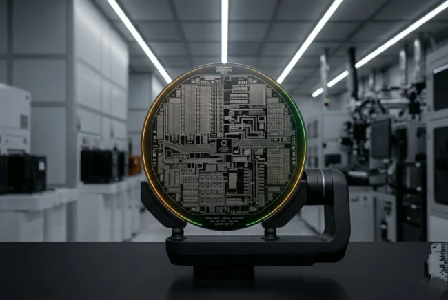
But beneath the patriotic fervor and the legitimate milestones lies a complex, highly technical reality that is often entirely misunderstood by the mainstream. When consumers hear “semiconductor,” they immediately think of the processor powering their ultra-flagship smartphone—the 2nm Snapdragon or the Apple A-series.
India is not fabricating those chips today. We will not be fabricating them next year, and we likely won’t be fabricating them before the end of the decade.
This is not a failure; it is a masterstroke of pragmatic industrial policy. Here is the reality check on India’s ‘nm’ (nanometer) journey, why we are deliberately avoiding the smartphone processor race, and why mastering the “boring” chips is the only mathematical way to win the semiconductor marathon.
The “nm” Obsession Explained
To understand why India isn’t printing smartphone chips, we have to strip away the marketing jargon surrounding the “nanometer” metric. Historically, the nm node (e.g., 28nm, 5nm, 2nm) referred to the physical length of a transistor gate. Today, it’s mostly a marketing term used to denote a generation of manufacturing technology. Smaller nodes mean denser transistors, higher performance, and vastly better energy efficiency.
The global semiconductor market is fiercely divided into two categories:
To put it bluntly, you do not need a $30,000 2nm wafer to tell a washing machine when to spin.
The Dholera Reality Check: Embracing 28nm
The crown jewel of India’s current silicon push is the ₹91,000 crore ($11 Billion) Tata Electronics fabrication plant in Dholera, Gujarat, developed in partnership with Taiwan’s PSMC and utilizing equipment from the Dutch lithography giant ASML.
When this plant rolls out its first silicon in late 2026 or early 2027, it will not be competing with TSMC’s 2nm lines. Instead, it is explicitly targeting the 28nm to 110nm nodes.
Why? Because 28nm is the absolute “sweet spot” of the global supply chain.
During the infamous 2021-2023 chip shortage that paralyzed the global automotive industry, companies weren’t waiting on 3nm smartphone processors; they were desperate for 28nm microcontrollers. As the world transitions to Electric Vehicles (EVs) and smart industrial automation, the demand for mature nodes is skyrocketing. By targeting 28nm, India is strategically inserting itself into a highly profitable, high-volume market segment that directly supports the products India actually manufactures—cars, two-wheelers, consumer electronics, and industrial equipment.
The Mathematics of Maturity
| Feature | Mature Nodes (28nm-110nm) | Cutting-Edge Nodes (2nm-5nm) |
|---|---|---|
| Average Wafer Cost | ~$3000 – $4000 | ~$28000 – $35000 |
| Primary Use Cases | Automotive MCUs, IoT, Display Drivers, Power | Smartphone SoCs, AI Accelerators, HPC |
| Capital Expenditure | High, but attainable | Astronomically high (requires EUV) |
| Global Market Share | Highly distributed | ~92% controlled by TSMC (Taiwan) |
The Sub-5nm Wall: Why We Aren’t Making Smartphone Chips
So, if India has the capital and the political will, why not just leapfrog straight to 2nm and challenge TSMC or Samsung for the smartphone market? Because leapfrogging in semiconductor fabrication is financial and structural suicide.
1. The EUV Monopoly
To fabricate anything below 7nm, you must use Extreme Ultraviolet (EUV) lithography. A single EUV machine from ASML costs hundreds of millions of dollars, requires several Boeing 747s to transport, and takes months to calibrate. Operating these machines requires a level of institutional knowledge and precision that a first-generation fab simply does not possess. Tata’s Dholera plant is correctly relying on mature Deep Ultraviolet (DUV) tools first. You have to learn to walk before you can sprint at the speed of light.
2. The Infrastructure Paradox
Advanced silicon fabrication is the most unforgiving manufacturing process in human history. A 2nm fab requires completely uninterrupted, hyper-stable electricity. A millisecond voltage sag can destroy millions of dollars worth of wafers. It also requires millions of liters of ultra-pure water daily. While India is rapidly upgrading its industrial parks to provide this “plug-and-play” stability, the ecosystem is not yet bulletproof enough to risk a $20 billion advanced node gamble.
3. The Missing Connective Tissue
Fabricating the chip is only one part of the puzzle. Once a chip is printed on a wafer, it must be sliced, packaged, and tested—a process handled by OSATs (Outsourced Semiconductor Assembly and Test).
We are currently building the packaging ecosystem. Micron’s Sanand plant and CG Power’s automotive packaging facilities are scaling up right now in 2026. Until our domestic OSAT ecosystem is fully mature, printing advanced 2nm logic chips domestically is putting the cart before the horse.
India’s Secret Weapon: The Talent Paradox
Perhaps the most frustrating irony of India’s semiconductor journey is that we actually do make smartphone chips—just not on our own soil, and not under our own IP.
Roughly 20% of the world’s semiconductor design engineers are Indian. When Qualcomm tapes out a new Snapdragon processor, or ARM designs a 2nm architecture, Indian engineers in Bengaluru, Hyderabad, and Pune are doing the heavy lifting. We have completely mastered the “Fabless” layer of the industry (designing the chip architecture).
The ultimate goal of the India Semiconductor Mission isn’t just to pour concrete and build factories; it is to shift from exporting talent to owning Intellectual Property. By establishing domestic 28nm fabs, we give our massive pool of local chip designers a physical place to test, iterate, and manufacture their own proprietary silicon for the domestic market.
The Verdict: Winning the Marathon
If you measure India’s success by whether or not we are printing the processor inside the next iPhone, you are looking at the wrong scoreboard.
The reality of India’s ‘nm’ journey in 2026 is one of calculated, structural realism. We are deliberately stepping out of the brutal, hyper-expensive 2nm smartphone race dominated by TSMC. Instead, we are quietly building the foundational infrastructure—OSAT packaging plants, compound semiconductor facilities, and 28nm mature fabs—that the rest of the physical world desperately needs to function.
We aren’t fabricating smartphone chips yet because we are too busy building the ecosystem that will ensure we never face a supply chain crisis again. In the high-stakes game of global silicon, boring and reliable is exactly how you win.