Tata Electronics vs Micron: Who is Winning India’s Semiconductor Infrastructure Race?
If you observe the Indian technology sector in mid-2026, it is impossible to ignore the massive influx of capital pouring into the domestic semiconductor ecosystem. The India Semiconductor Mission (ISM) has transitioned from a localized policy paper into a sprawling, multi-billion-dollar physical reality. Billboards across Gujarat proudly display the logos of the two undisputed titans leading this charge: Micron Technology and Tata Electronics.
For casual observers and financial analysts alike, it is tempting to view this as a head-to-head race. Who is building faster? Who is investing more? Who is “winning” the race to make India a global semiconductor superpower?
The reality is vastly more complex, highly technical, and completely synergistic. While both companies are laying the concrete for India’s silicon future in the state of Gujarat, they are occupying entirely different ends of the semiconductor supply chain. Here is the definitive, deep-dive breakdown of the Tata Dholera mega-fab, the newly operational Micron Sanand facility, and why comparing them is like comparing a printing press to a bookbinder.
Micron Sanand: The Speed of ATMP Execution
If the metric for winning is “speed to market,” then Micron Technology has already crossed the finish line. On February 28, 2026, Prime Minister Narendra Modi officially inaugurated Micron’s Assembly, Test, Marking, and Packaging (ATMP) facility in Sanand, marking the commencement of India’s first commercial semiconductor operations.
The ATMP Reality
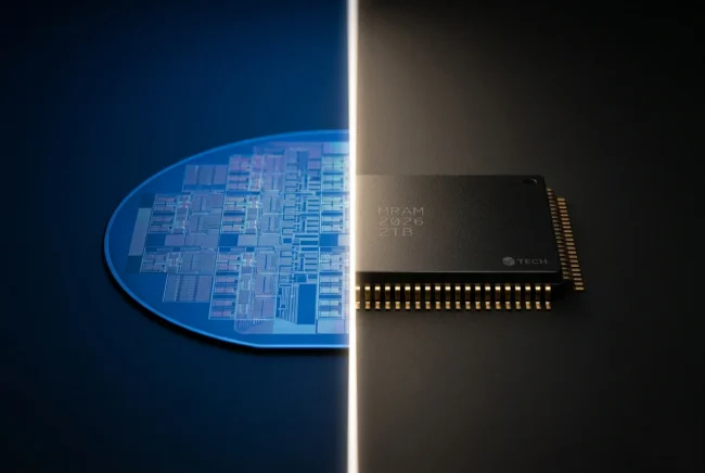
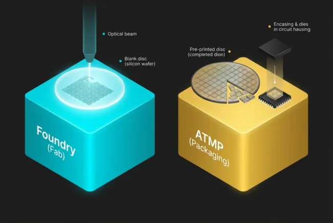
To understand Micron’s victory, you must understand what the Sanand facility actually does. It is an ATMP plant (often referred to interchangeably as an OSAT—Outsourced Semiconductor Assembly and Test)
Why Micron Moved First
ATMP facilities require a fraction of the time and capital to build compared to a full foundry. The Sanand plant represents a $2.75 billion combined investment, and by utilizing pre-existing industrial infrastructure, Micron went from signing the Memorandum of Understanding (MoU) in June 2023 to commercial production in under three years. This blistering pace gives India an immediate, tangible foothold in the global supply chain, serving as the critical “backend” required to support the AI and data center boom.
Tata Dholera: The Foundry Behemoth
If Micron represents the backend packaging, Tata Electronics represents the absolute foundational bedrock. Located in the Dholera Special Investment Region (SIR), Tata’s massive ₹91,000 crore ($11 Billion) fabrication plant is playing a much longer, vastly more complex game.
The True “Fab” Experience
Unlike Micron’s Sanand plant, the Tata Dholera facility is a True Foundry (Fab). This means it takes raw, blank silicon discs and physically prints billions of microscopic transistors onto them.
The Value Chain: Printing vs. Packaging
To truly grasp why the “Tata vs. Micron” narrative is a false dichotomy, we must look at the mathematical and technical differences in their respective operations.
| Metric | Micron (Sanand) | Tata Electronics (Dholera) |
|---|---|---|
| Facility Type | ATMP (Assembly, Test, Marking, Packaging) | Foundry / Fab (Silicon Wafer Fabrication) |
| Current Status (Mid-2026) | Fully Operational / Commercial Production | 50% Constructed / Trial Production Late 2026 |
| Primary Output | Packaged DRAM and NAND memory modules | 28nm – 110nm logic and power management chips |
| Total Investment | ~$2.75 Billion USD | ~$11 Billion USD (₹91,000 crore) |
| The Primary Challenge | Advanced thermal packaging & precise testing | Lithography calibration & extreme cleanroom stability |
A semiconductor foundry (Tata) is arguably the most complex manufacturing environment on the planet. It requires flawless power grids, millions of liters of ultra-pure water, and environments that are thousands of times cleaner than a hospital surgical theater. A single speck of dust can ruin a $10,000 wafer. Because of this unforgiving physics, a Fab inherently takes years longer to build and calibrate than an ATMP facility.
The Ecosystem Synergy: Why India Needs Both
The India Semiconductor Mission (ISM) is not funding these projects in isolation; they are highly calculated puzzle pieces designed to fit together.
Historically, the semiconductor supply chain has been hopelessly fragmented. A chip might be designed in California, printed in Taiwan, shipped to Malaysia for packaging, and finally sent to China to be placed into a smartphone. This fragmentation caused the catastrophic supply chain failures of 2021.
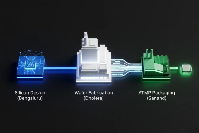
India is attempting to build the entire vertical stack within its own borders.
By having both Tata and Micron operating within the same geographic corridor in Gujarat, India drastically cuts down the logistics cost and time-to-market for final electronic products.
The Verdict: Two Different Marathons
So, who is winning India’s semiconductor infrastructure race?
Micron is the undisputed winner of the short game. By leveraging their global expertise to rapidly deploy an ATMP facility, they gave the Indian government a massive, tangible victory in 2026. They proved to the global market that India is capable of handling delicate, high-tech silicon operations, shipping finished products directly to global OEM giants like Dell.
Tata Electronics, however, is the anchor of the long game. Building a foundational 300mm foundry from the ground up, securing ASML lithography tools, and establishing a domestic supply of mature node logic chips is the ultimate endgame of semiconductor sovereignty. When Dholera boots up its trial production later this year, it will fundamentally change India’s import reliance for automotive and industrial silicon.
They are not competing against each other. Micron is building the roof, Tata is pouring the foundation, and together, they are constructing an industrial fortress that will define India’s economic trajectory for the next fifty years.