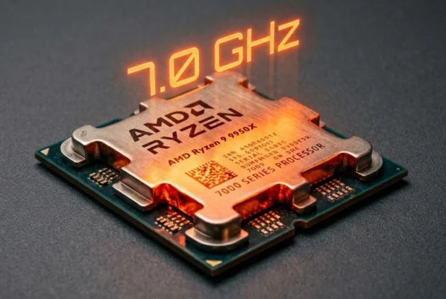
7GHz Speeds Leaked: Is the AMD Zen 6 Actually Worth the Wait?
The desktop processor market has settled into an uneasy truce following the launch of AMD’s Zen 5 architecture. While the Ryzen 9000 series delivered impressive efficiency and solid IPC (Instructions Per Cycle) gains, the raw clock speed advancements felt somewhat conservative. However, new supply chain leaks and engineering benchmarks suggest that AMD’s subsequent architecture, Zen 6 (codenamed “Medusa”), is abandoning conservative efficiency in favor of brute-force frequency scaling and massive architectural overhauls.
Rumors of AMD breaching the 7.0GHz barrier have ignited the enthusiast community. But with a projected release window slipping into late 2026 or early 2027, builders are facing a difficult choice: build now on the mature Zen 5 platform, or endure the wait for a potentially historic generational leap.
Here is a comprehensive breakdown of the leaked specifications, the architectural shifts, and whether Zen 6 is genuinely worth delaying your next PC build.
The Pursuit of 7.0GHz: Clock Speeds and Node Jumps
The most sensational claim surrounding Zen 6 is the aggressive pursuit of ultra-high frequencies. While reaching 7.0GHz out of the box may be an extreme lab target, the fundamental shift in manufacturing processes guarantees a massive uplift over current hardware.
The TSMC 2nm Leap: Unlike Zen 5, which utilized a refined 4nm node, Zen 6 CCDs (Core Complex Dies) will be fabricated on TSMC’s bleeding-edge N2P (2nm) process. This allows for a dramatic reduction in transistor gate size, enabling much higher frequencies at equivalent power draws.
Target Frequencies: Reliable industry insiders indicate that standard Zen 6 engineering samples are already easily achieving 6.3GHz to 6.4GHz boost clocks. This is a massive 10% to 15% increase over the absolute peak of the current Ryzen 9 9950X (which boosts to 5.7GHz).
The 7GHz “Halo” Tier: While standard consumer SKUs will likely hover around the 6.5GHz mark, specialized “Black Edition” or highly binned SKUs are reportedly being tested internally with a 7.0GHz target. Whether this requires exotic cooling or massive power limits remains to be seen, but the silicon is theoretically capable.
IPC Enhancements: Clock speeds are only half the equation. Leaked technical documents confirm that Zen 6 will also feature a 10% to 15% IPC (Instructions Per Clock) uplift over Zen 5, largely driven by wider execution engines and an overhauled front-end prediction algorithm.
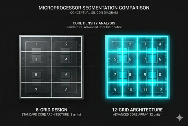
The 12-Core CCD: Redefining Density and Cache
For several generations, AMD has relied on the 8-core CCD configuration. Zen 6 shatters this limitation, fundamentally changing how Ryzen CPUs will scale in multi-threaded workloads.
50% More Cores Per Die: The new Zen 6 CCD will house 12 cores instead of the traditional 8. This means a dual-CCD flagship consumer processor (e.g., the potential Ryzen 9 10950X) will feature 24 physical cores and 48 threads without requiring a physically larger package.
Massive L3 Cache Expansion: To feed these additional cores, the standard L3 cache per CCD is increasing by 50%—jumping from 32MB to 48MB per die. For a dual-CCD processor, that equates to 96MB of L3 cache before even factoring in the X3D variants.
Die Size Efficiency: Astonishingly, due to the density of TSMC’s 2nm node, these 12-core, 48MB cache CCDs will measure approximately 76 mm². This is only marginally larger than the 8-core Zen 5 CCDs (~71 mm²), ensuring excellent yield rates and maintaining compatibility with existing physical substrate dimensions.
The I/O Die Upgrade: The central IOD (Input/Output Die) is also getting a shrink, moving from the aging 6nm process to TSMC’s advanced 3nm (N3P) node. This will drastically reduce idle power consumption, improve memory controller stability for higher-speed DDR5, and potentially house integrated RDNA 3.5 or RDNA 5 graphics architectures.
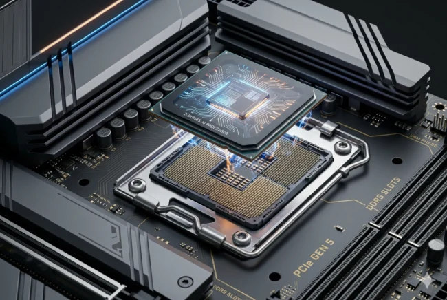
Platform Longevity: The AM5 Survival
One of the most critical factors for PC builders is socket longevity. Fortunately, the latest leaks provide immense relief for early adopters of the current platform.
AM5 is Safe (For Now): Despite the massive architectural changes and the shift to 2nm silicon, AMD has reportedly confirmed to motherboard partners (like ASUS and ASRock) that Zen 6 will be fully compatible with existing AM5 motherboards.
BIOS Updates Required: While physically compatible, exploiting the full 24-core density or the highest memory speeds will likely require high-end X870E or B850 boards with robust VRMs, along with a massive 32MB or 64MB BIOS update.
The AM6 Horizon: Supply chain whispers suggest that Socket AM6 will not arrive until 2028, likely debuting alongside the Zen 7 architecture to introduce PCIe 6.0 and DDR6 memory standards. Therefore, Zen 6 represents the final, most powerful iteration of the AM5 era.
Cooler Compatibility Retained: Because the physical package dimensions and IHS (Integrated Heat Spreader) thickness must remain identical to fit the AM5 socket, your current high-end AIO liquid coolers or premium air coolers will mount perfectly to Zen 6 processors.
The Competition: Zen 6 vs. Intel Nova Lake
AMD does not exist in a vacuum, and the sheer scale of the Zen 6 upgrade is a direct response to Intel’s terrifyingly powerful 2026 roadmap.
The 52-Core Threat: As we covered previously, Intel’s upcoming Nova Lake architecture features a dual-compute tile design capable of up to 52 cores and a massive 700W power draw limit. Zen 6 is AMD’s leaner, more efficient counter-punch.
Cache Wars: Intel is introducing its “bLLC” massive cache system to combat AMD’s X3D dominance. In response, AMD’s strategy with Zen 6 is to raise the base cache to 48MB per CCD, ensuring that even non-X3D variants can handle immense rendering and gaming pipelines without latency penalties.
Efficiency vs. Brute Force: While Intel appears to be abandoning thermal limits to reclaim the multi-threaded crown, AMD is relying on the superiority of the TSMC 2nm node to deliver 24 cores at a fraction of the wattage, appealing to builders who don’t want to invest in 420mm custom water loops.
The Verdict: Is Zen 6 Worth the Wait?
If you are currently running a Ryzen 5000 or early Ryzen 7000 series CPU, the decision is nuanced.
If you are a professional who relies on multi-threaded rendering or localized AI workloads, waiting for the 24-core Zen 6 flagship in early 2027 is the strategically sound choice. The combination of 2nm efficiency, 12-core CCDs, and massive base cache expansions represents a true architectural leap rather than a mere iterative refresh.
However, if you are strictly a gamer looking to maximize frames right now, the current Zen 5 X3D chips (like the Ryzen 7 9800X3D) will saturate any modern GPU on the market. There is no need to suffer through a year and a half of bottlenecking just to chase the mythical 7.0GHz dragon.
Build your AM5 system today with a solid motherboard, enjoy the current generation, and rest easy knowing that when Zen 6 finally drops, a simple BIOS update will unlock the most powerful silicon AMD has ever created.